

All of us encounter issues which have a means of mildly frustrating us. Enough to bug us, however just not sufficient to go out of our technique to appropriate. It could be a sticky lock in determined want of a spray of WD-40, a weed rising in the course of the sidewalk, or a dusty tabletop. For a while this annoying thing for me was a coat closet in the middle of the house with none light in it. Having two dogs that generally forget footwear are usually not chew toys, this closet has change into the convenient residence to our shoe collection. As time went on more footwear accumulated and the second legislation of thermodynamics held true – the closet grew to become a dark, disorderly mess. I have wished to take a stab at etching a PCB for a while. This appeared like the perfect opportunity to check out this new methodology. The circuit would not be difficult so I could also shine some mild on others (in addition to my closet) who may be contemplating this for the first time. This mission particularly requires LEDs, resistors, printed circuit board a change and pcb assembly a few type of battery. The objective is to make use of a normally closed change to maintain the LEDs off when the door is shut and to turn them on as soon as the door is opened. Sketch out a circuit. Track down all required components. Remember to do your Ohm’s Law test to verify all elements are sufficiently rated. In my case, I found the present going by way of each LED on fully charged 18650 cell (my battery of selection) could be a tad excessive. However, I decided to continue with this set up to forestall the LEDs from getting too dim because the cell dies. Plus, I had a plethora of one hundred Ω resistors leftover from a earlier mission that had been simply ready to have a goal! Using a good PCB Design platform can save lots of time while designing the format of your PCB. Programs comparable to Eagle and EasyEDA allow you to design your schematic then build directly from this schematic. Here is more info on printed circuit board guide stop by our website. This ensures part sizes and connection factors are accurate and accounted for on the PCB. Another timesaver of this software program is the autorouter device. This will lay out all traces in paths that only interfere with components and different traces which might be connected. After the PCB has been laid out and the circuit connections have traced, confirm the circuit one last time prior to printing. Be certain that to print using a 1:1 scale so the format dimensions are correct. To make sure an accurate transfer, tape this print out over high of a copper clad laminate PCB. Using a pushpin, stab by way of the paper where each part lead will penetrate the board. This may go away dots on the copper the place these components go. The small indentation on the copper will even help the drill bit discover the precise location the lead will go. Remove the printed sheet. Make sure that all components are marked on the copper. Use a 1/32″ (most) bit to drill out the holes that were marked on the board. Once all the holes are drilled, clean the highest of the copper plate with a bit of sandpaper. Using a everlasting marker, draw to traces between all of the parts referencing the printed PCB layout. Allow a while for the ink to dry. Touch up the board the place the marker is faint. Once the second coat of marker is totally dry it’s time to give the board a bath in ferric chloride. Ferric chloride is a corrosive, acidic chemical compound that can eat away all copper on the board that isn’t protected by the marker’s ink. Pour a modest quantity of ferric chloride into a plastic container with a lid; simply enough to cowl the board completely. Let the board soak for 10 minutes, be sure the lid is properly secured and agitate it every few minutes by rocking the container back and forth. After 10 minutes inspect the board and if no copper is visible, remove the board whereas carrying a latex glove. Pat the board dry with a disposable rag to take away all ferric chloride from the board. Rinse the board with acetone that can make fast work of the marker ink to reveal your unharmed traces. The etching course of is full! After the board has been etched, use a multimeter to do a continuity test. Be certain all traces have been successful and likewise start and terminate in the proper locations earlier than making use of energy to the circuit. Once all traces have been verified, add the components to their appropriate position and solder them in. Apply voltage and watch in awe as your completely etched circuit capabilities precisely as planned! To finish my mission I will attach the 18650 holder to the backside of the PCB and mount the assembly inside my closet. The switch has usually closed contacts so that when the door is closed the change will probably be pressed, the contacts will be open, and the lights will be off. When the door is opened the change will not be pressed, the contacts can be closed and the light will be on! Chris Font has left Hallam-ICS to pursue different endeavors, however his contributions to the corporate proceed to be valued. Hallam-ICS is an engineering and automation company that designs MEP methods for services and plants, engineers management and automation options, and ensures security and regulatory compliance via arc flash research, commissioning, and validation. Our places of work are positioned in Massachusetts, Connecticut, New York, Vermont and North Carolina and our tasks take us world-vast.
Stanford Release Instructions To Construct A Black Mirror-Model Robot Dog
The popular show ‘Black Mirror’ may be on hold due to the pandemic spreading across the globe, however followers of the dystopian world can create a part of the sci-fi series on their own. A Stanford pupil built a robotic canine similar to that used in the episode titled ‘Metalhead’ that hunts and kills humans in an apocalyptic setting. The miniature version, printed circuit board called the Stanford Pupper, was developed using a 3D printer, a PlayStation controller and other common items – and the team has shared all the main points for the public to make use of. It has 12 levels of freedom, meaning it will probably goes backwards, forwards, side-to-aspect and PCB board assembly also features a ‘sneaky mode’ that mimics the motion of a real canine creeping on the floor. A Stanford student constructed a robotic canine just like that used in the episode titled ‘Metalhead’ that hunts and kills humans in an apocalyptic setting. ‘We’re a scholar robotics crew at Stanford and we had been impressed by other quadrupeds and other legged robots that we’re seeing on the market like Boston Dynamics,’ Nathan Kau, one of the creators, stated throughout an interview. ‘But we actually wish to play and have one in our personal fingers, and we didn’t have a method to do this because they are very costly. ‘That led to utilizing inexpensive parts whereas finding probably the most powerful motors, powerful actuators and doing the software program ourselves. The three-pound machine is ready to trot, hop, run and sneak throughout the floor like a residing dog – and can be made for pcb assembly $600 to $900. To create a mini ‘Metalhead’, you have to a range of items together with carbon fiber plates for the robot’s body and a Raspberry Pi. ‘You should buy many of the parts straight from a reseller like Amazon or McMaster-Carr, however for some you’ll must get them customized manufactured for you,’ reads the directions. ‘The custom components include the carbon fiber routed elements, the 3D printed parts, the ability distribution Printed Circuit Board (Www.Video-Bookmark.Com), and the motors. Build time is about four to 10 hours relying on how skilled you are at constructing a robot, however the scholars note that it’s just like constructing a quadcopter drone. Black Mirror’s ‘Metalhead’ was the fifth episode of the fourth season that was filmed completely in black and white. The story follows a character named Bella by a world ravaged by robotic canines that have taken over after the collapse of human society. And the machines pulled inspiration from Boston Dynamic’s robots. The creator of Black Mirror, Charlie Brooker, recently announced he can be taking a break from writing another series, as the general public would battle to ‘stomach’ the show in the midst of the global pandemic. In the mean time, I do not know what stomach there could be for tales about societies falling apart, so I’m not working away on one of those,’ he stated in an interview with Radio Times. I’m kind of keen to revisit my comic skill set, so I have been writing scripts aimed at making myself giggle.
Printed Circuit Board Design, Diagram And Assembly
Printed Circuit Board Design, Diagram and Assembly Process. Printed Circuit Board Design or Printed Circuit Board (PCB) or Printed Wiring Board (PWB), is a board made out of insulating and extremely heat-resistant insulating materials reminiscent of fiberglass. These boards are also called substrates. A substrate or board could have only one single layer (single-layer circuit board) or more than one layer (multilayer circuit board). A conductive metal comparable to copper is used to make conductive pathway or traces to facilitate flow of electricity. Once these conductive traces are etched on the substrate, it’s termed as “printed circuit board”. How to draw a Circuit Diagram? The history of circuit boards dates again to mid-nineteen thirties, when an Austrian engineer Paul Eisler invented the PCB whereas designing a radio set. These radio sets were later massively utilized in World War II by United States. After this, the use and software of circuit boards as a result of industrial in Electronic Companies. These circuit boards are of no good use till digital parts are soldered. Electronic parts may be both by means of-gap or SMD. Again the technology used to solder these components on the circuit board can be via-gap expertise or Surface Mount Technology. Soldering material might embrace solder in the type of solder wire, solder paste, solder balls for BGA (Ball Grid Array) and soldering flux. As explained above, a printed circuit board is a board made of one or more layers of insulating PCB Material (fiberglass, ceramic, highly heat-resistant plastic or every other dielectric materials) with conductive pathways etched with conductive steel equivalent to copper. Throughout the PCB Manufacturing Process, traces of copper or any other conductor is etched off the board leaving only traces which can be wanted to mount / solder digital parts. Once all Basic Electronic Components are soldered on the circuit board and the board is ready to be used, it is named Printed Circuit Assembly (PCA) or pcb assembly Printed Circuit Board Assembly (pcba [just click the up coming website]). The present generic normal for printed circuit board design is IPC-2221A. IPC 2221A generic standard on printed circuit board design gives rules for manufacturing circuit boards and quality tips. These information and pointers is relevant for all Kinds of PCB including Single-Layer PCB and Multilayer PCB and data consists of substrate info, material properties, standards for floor plating, conductor thickness, element placement, dimensioning and tolerance guidelines and more. Other circuit board designing requirements are IPC-2220 and IPC-9592. It needs to be famous that IPC and different requirements will present info on the right way to correctly route the board. For an ideal and reliable circuit board design, good knowledge and understanding of PCB structure techniques and primary understanding of circuit operation is required. While designing a printed circuit board prototype, one should take proper care of the substrate materials based of kind of soldering know-how and parts to be used. The width of the traces of the circuit board (circuit conductors) ought to be chosen properly primarily based on anticipated most temperature rise at the rated current and acceptable impedance. Other factors to keep in mind with printed circuit board design are CTE, price and dielectric properties. The designer must carefully steadiness the constraints of price with reliability and efficiency wants. In addition, solder mask and by way of holes should also be selected rigorously. A circuit diagram is a diagram showing and explaining how and the place electronic components will probably be mounted to attain the goal product. Each component on a circuit board diagram is represented by a circuit image. Making a circuit diagram previous to production is vital. It gives an thought of how the circuit will work. How to realize the target product. A circuit diagram is essential for any new digital product, machine or gadget. How to attract a Circuit Diagram? Drawing a circuit diagram shouldn’t be that troublesome if you already know the basics. 1. Learn and perceive all of the common symbols and abbreviations for electronic elements for use on the diagram. 2. Using a ruler, draw connecting wires as straight lines. Negative provide is usually labeled 0V, zero volts. 3. For advanced circuit diagrams, begin from left to right. So that indicators circulate from left to right (inputs and controls should be on the left, outputs on the precise). Mounting electronic elements on the circuit board. Getting it prepared to be used is what is called circuit board meeting. A Circuit Board Assembly Process might use by means of-hole meeting expertise or floor mount know-how (SMT) or a mix of each. Once the circuit board is assembled with elements it’s prepared for testing. Finally to be assembled with the product. But it is not assured that a circuit board assembly will give 100% zero defect manufacturing. There will probably be defects. These defect should be reworked / repaired.
PCB (printed Circuit Board) Parts And Components Identification – Fully4world
A printed circuit board (PCB) mechanically supports and electrically connects electronic components or electrical components using conductive tracks, pads and different options etched from one or more sheet layers of copper laminated onto and/or between sheet layers of a non-conductive substrate. Components are typically soldered onto the PCB to both electrically connect and mechanically fasten them to it. Printed circuit boards are used in all however the only electronic merchandise. They’re additionally utilized in some electrical merchandise, comparable to passive switch packing containers. Resisters limit the circulation of present through a circuit. These small, horizontal cylinders typically bear 4 or five colored stripes that help establish their resistance and tolerance. Larger resistors may have this info written on them as properly. Their schematic programs can also have this data printed in words as well. In both case, PCBs use R to note resistors.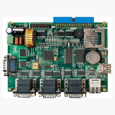 Transistors are a specific sort of swap. You possibly can identify them by their three terminals and their “D” form. Circuit boards often use Q to indicate transistor locations. Transistor diagrams are circles with three leads. Contained in the circle, one level goes directly to a bar, whereas the opposite leads branch off diagonally from the bar with considered one of them containing an arrow. Relays are electronic switches. Powered relays are open whereas disconnected relays are closed. These components typically have plastic shells with their specification written on them. Most boards use “K” to label relays. Transformers are usually fairly easy to identify by sight, and many have their specs printed on them. They are sometimes marked with an “T” on a circuit board. A swap is a element which controls the open-ness or closed-ness of an electric circuit. They allow management over present flow in a circuit (with out having to actually get in there and manually minimize or splice the wires). Switches are important elements in any circuit which requires consumer interaction or management. These variable resistors are usually marked in ohms utilizing three digits. The primary two digits are the numerous figures with the third proving the power of 10 multipliers. Potentiometers even have a letter code to point the resistance change, and a VR for variable resistor marked on them somewhere. These full circuits-on-a-chip will take some effort to identify correctly, as several various kinds of ICs can are available in the same bundle. Marked as U or IC on most circuit boards, you usually must search for the device’s datasheet to seek out the data. Datasheets supply a schematic of their gadgets. Are usually discovered on-line. Circuit diagrams use rectangular blocks to signify these components. Essentially loops of wire, inductors are sometimes difficult to determine. You can find them either as a uncooked wired coil or coloration coded. In both case, it is best to check the parts earlier than using them. Fortunately, PCBs use an L to point an inductor. In electronics and electrical engineering, a fuse is an electrical security device that operates to offer overcurrent protection of an electrical circuit. Its important element is a metallic wire or strip that melts when too much current flows by means of it, PCBA thereby interrupting the present. It’s a sacrificial system; once a fuse has operated it’s an open circuit, and it must be changed or rewired, depending on type. If you are you looking for more regarding pcba – http://Www.Authorstream.com, have a look at our own internet site. Diodes one-method electrical parts with a band that indicated the present course. You’ll find their specs on their shells. You may additionally come across LEDs. Zener diodes as well. Diagrams use an arrowhead and a bar to indicate diodes whereas circuit boards use D or CR. The arrow points in the route of the current. Marked on boards with an X or Y, these pure clocks keep our electronic devices working easily and on time. The unique appearance of a crystal oscillator makes these parts the best to establish. They even have their specification written on them. Capacitors store electric charge. These components come as small disk-formed gumdrops or massive cylinders. In either case, the knowledge is printed straight onto them. PCBs, use C to make capacitors. A Bridge rectifier is an Alternating Current (AC) to Direct Current (DC) converter that rectifies mains AC input to DC output. Bridge Rectifiers are widely utilized in power supplies that provide vital DC voltage for the digital parts or devices. They are often constructed with four or more diodes or another managed stable state switches. Depending on the load present requirements, a correct bridge rectifier is selected. Components’ ratings and specifications, breakdown voltage, temperature ranges, transient present score, forward present rating, mounting requirements and different issues are taken into account while choosing a rectifier energy provide for an appropriate digital circuit’s application. A LED, or PCBA mild emitting diode, is a component that can give off light. You will discover them in single and multi-color and low and high-power varieties. Low-energy, single colour LEDs are the most common. They often come in their respective colors, but not all the time. They may only have two terminals, a cathode, and an anode. Multi-coloration ones have multiple shade. A set of terminals for every coloration. High-power LED has a big steel casing to dissipate the extra heat. LEDs use the diode image on diagrams.
PCB Assembly Services
We provide fast-flip prototype, PCBA low-volume and production PCB assembly with surface-mount (SMT), via-hole (THT) and combine components. If you have any type of questions relating to where and how you can utilize printed circuit board (click through the up coming webpage), you could contact us at our own web site. We provide turn-key (just send us the Gerber and BOM information), consignment (you provide all elements) and various parts purchase options that will help you scale back value and wait time. Our fast-flip prototyping service can assemble your boards within 24 hours. We can handle small quantity as well as volume productions. All our companies are at a really aggressive worth. With 100% satisfaction assure. We provide both Prototype. Production PCBA companies. For Prototype, there is no such thing as a limitation in amount. Reference pricing are based on the number of pins and component varieties. 0.025 per pin for DIP, TH components. When all of the elements and parts are prepared, the lead time can be as brief as 24 hours. Weekend flip-around could be arranged. We can even present just-in-time assembly to fill your provide pipeline. To assemble your PCB board, we settle for components and elements in the next three approaches. 1. You provide the components. 2. We buy in your behalf, out of your specified distributors, similar to Digi-Key, Mouser, printed circuit board Arrow, Future Electronics and others. 3. Use our in-house part inventory. Components on your PCBA venture may be supplied in any a number of approaches above. We order real elements out of your designated suppliers or our companion corporations including DigiKey, Mouser, Arrow, Avnet, Future Electronics, Bell Micro, Newark and TTI. To help shopper obtain higher pricing on volume, we offer free spare elements parking. We inventory your spare parts freed from cost on your future orders. We are within the process of creating a components change program which allows clients to commerce spare elements. These embrace resistors (all type, dimension and worth, full stock), capacitors, diodes, transistors, LED, frequent IC and connectors. Manual soldering for special components, e.g. wires and temperature sensitive elements. We carry out multiple quality assurance procedures before delivery out any board. Functional test (take a look at modules should be provided) . We may accommodate particular requirements and new applied sciences. Please inquire in case you have other needs. We’re more than pleased to work out the answer with you. Finished boards are packed in antistatic bag with unit-pack or a number of-pack field. Copyright © 2002 – 2022 MyRO Electronic Control Devices Inc. All rights reserved.
PCB Assembly Considerations
Decisions about element selection and structure composition can increase meeting costs and the time-to-market. PCB assembly issues contain making careful design selections. Modern EDA software program capabilities can reduce PCB assembly points. PCB assembly considerations include deciding on quality components, choosing the right layout, and leveraging EDA software program capabilities. When taking a look at the results of various surveys about why electronic products fail in the marketplace, a number of trends become apparent. In some situations, design groups attempt to unravel non-existent problems or over-design a product with the assumption that customers need extra features. The choice to over-design could trigger them to run over price range and pcb assembly encounter supply chain issues. This concern illustrates the need for PCB board (www.linkagogo.com) designers to fastidiously contemplate important PCB assembly issues. Design for assembly principles earlier than they soar into the fabrication course of. The selection of high quality elements, the appropriate layout, and EDA software program can mean the difference between a profitable project or a pricey failure. PCB assembly can fall prey to the same issues that prevent good ideas from turning into profitable products. To keep away from these issues, design teams should apply the principles behind design for meeting (DfA). Considering DfA ideas when assembling a PCB will ensure design groups make considerate choices that decrease the lead time wanted for a mission, reduce risk, and mitigate points that may end up in expensive revisions. Design for meeting affects how designers select elements, select suppliers, and work with fabricators. Additionally, DfA drives selections relating to PCB layouts. DfA rules involve making PCB design choices about performance, efficiency, and price, and every factor has a direct influence on the form, high quality, and reliability of the completed product. The primary goal of DfA is ease-of-assembly. Moving in direction of that goal requires an emphasis on eliminating complexity and reducing uncertainty. An emphasis on eliminating complexity pushes design groups to think about decreasing the number of components used for a PCB and to consider the type of components chosen. For instance, design teams might decide that choosing resistor or capacitor arrays-relatively than teams of single passive parts-saves board space and lowers prices. The “back-to-basics” approach to DfA also prompts design groups to consider-and perhaps reconsider-the usage of fragile, heavy, or bulky components. Heavy and bulky transformers, power resistors, and mechanical assemblies drive transport costs higher and require specific fabrication measures to make sure that the bodily design of the board helps the elements. Fabricators are assisted by the choice to cut back the number of elements, as fewer elements imply that fabricators require much less choose and place passes for his or her gear. The use of standardized, pcb assembly cost widespread parts additionally decreases the variety of reel modifications for fabricator tools. Although fabricators acknowledge that product design could require a special element bundle, the usage of unique packages can introduce delays within the production course of due to fabricator requirements for evaluating the PCB structure with datasheet footprints for each component. DfA requires consideration to selections about the PCB layout. Choosing to depend on vias-in-part pads or wire harness assemblies may provoke a ripple impact that impacts stability, time, and price. Because the reflow course of for through-in-element can allow tin to leak, fabricators take the extra time and cost to fill vias-in-component pads with epoxy. Rather than use wire harness assemblies that may enhance costs and lead time, design groups should consider modular designs or completely different interconnection options. If a PCB design stipulates wire bonding or conformal coatings, fabricators require mask drawings that show the areas designated for the finish or coating. An emphasis on normal elements eases issues about the flexibility of fabricators to procure elements. Many EDA software program packages include part libraries that connect the PCB design group with reliable manufacturers and recognized inventories. Modern EDA software additionally improves the consistency and clarity of Gerber information, meeting drawings, and Bill-of-Materials. This emphasis on consistency and readability reduces time-to-market by guaranteeing fabricators that documentation contains all design revisions. The potential of EDA software program to generate a BOM from the schematic. Should you loved this short article and you would want to receive more info concerning Pcb assembly Cost kindly visit the web site. Reference notes additionally speeds the meeting process. While fabricators continue to manually overview the BOM, the aptitude to eradicate incomplete, inaccurate, or missing part numbers or mismatches between part numbers and descriptions saves time and reduces costs. PCB assembly concerns include the choice of quality elements, a wonderful format, and quality EDA software-discover the assets you want for all of this and more on the PCB Design and Analysis overview web page. The latest products and solutions from OrCAD PCB Designer can make it easier to achieve your next great design. If you’re trying to be taught extra about how Cadence has the answer for you, talk to us and our team of experts. Cadence PCB solutions is an entire front to again design tool to allow fast and environment friendly product creation. Cadence allows customers accurately shorten design cycles to hand off to manufacturing via modern, IPC-2581 business normal.
Flexible Circuits Vs. Printed Circuit Board
It is not uncommon for many designers and engineers to think about a versatile circuit as a printed circuit board (PCB) that can bend. While it is true that a flex circuit and PCB carry out the identical electrical perform, the structural and mechanical differences are important, and never understanding them may end up in poor yields and area failures. It is vital to notice the different terminologies which are used in the electronics trade. Flexible circuits have been known as flex, flex circuits, versatile pcbs and flexible printed circuit boards. Printed circuit boards will also be referred to as PCB’s or simply hardboards. Let’s start by stating the obvious distinction: a flexible circuit can bend, fold and twist, a printed circuit board cannot. This key difference requires a flex to be manufactured with a special set of supplies, design rules and totally different manufacturing processes. If you adored this short article and you would such as to get even more info regarding PCBA (linked internet site) kindly see the web-page. Perhaps the largest difference is the supplies. Both printed circuit boards and versatile circuits have similar building: Within the case of a single sided circuit, the construction is dielectric base layer, adhesive layer; copper or conductive material layer and perhaps a protective overlay materials. For a printed circuit board the bottom layer tends to be rigid and normally comprises glass reinforcement, FR4 is probably the commonest materials. This gives the material excellent dimensional stability, thermal resistance and mechanical power, however little or no skill to bend. Flexible circuit base supplies are most commonly made from polyimide. The material has excellent flexibility properties, however it does not have the identical mechanical assist for parts and is less dimensionally stable vs. Since printed circuit boards don’t flex, the requirements on the adhesives are restricted to chemical and thermal properties. Alternatively, a flexible circuit has an additional requirement to permit bending. An adhesive that works effectively for a hard board, would crack or fracture in a flex utility. An adhesive for a flexible circuit needs to “stretch” a bit. The result’s that an adhesive for a flex will have totally different thermal, chemical and mechanical properties from adhesives used in PCBs. There are two primary varieties of copper film, Electro Deposited (ED) and Rolled Annealed (RA). The important thing difference is that RA copper is far more versatile. Is required in dynamic flex applications. ED copper does have some flexibility and may be utilized in some circumstances, and is almost exclusively used to supply rigid pcb’s. There can also be a HDED (high ductility) copper that is electro-deposited with a remedy that makes it extra versatile, but not quite nearly as good as RA. Considerations for copper are seldom a difficulty for a inflexible printed circuit board since it doesn’t require flexing. Copper selection in a flexible circuit can be essential to efficiency, each in dynamic flexing and flex to install applications. The before mentioned material variations create an entire set of added complexities in design and fabrication of a flexible circuit. Registration tolerances, chemical and thermal properties and a host of different components mean design specifications for a flex might be totally different vs. The important thing variations discussed on this weblog pertain to frequent constructions in flexible and laborious board circuits. Both are available in alternate supplies for particular functions. Most notably, flexible circuits can be found in adhesiveless constructions.
Malala Is MARRIED: Nobel Peace Prize Winner Reveals She Tied The Knot
Malala Yousafzai has shocked her thousands and thousands of supporters world wide by getting married in a small, moving ceremony at her Birmingham dwelling. The youngest ever winner of the Nobel Peace Prize, now 24, spoke of her excitement for the ‘journey forward’ after tying the knot with Pakistani cricket coach Asser Malik in a relationship that had been stored secret from the wider world. The happy day comes more than nine years after she survived being shot within the face by the Taliban after she campaigned for ladies to go to school. Malala shared sweet photographs from the Nikkah – Islamic marriage ceremony – where she wore an attractive pink bridal outfit. She is seen smiling next to her new husband, who wore a matching pink tie, printed circuit board news in adorable outside snaps. While one other picture exhibits Malala touching her hair as Asser signed the wedding contract. Malala captioned the pictures: ‘Today marks a precious day in my life. Asser and that i tied the knot to be companions for life. We celebrated a small nikkah ceremony at dwelling in Birmingham with our families. Please send us your prayers. Malala and her new husband gaze into every others eyes in the stunning photos from their Nikkah: ‘Today marks a valuable day in my life. Malala and her new husband Asser Malik pose for a picture on their wedding day along with her father Ziauddin Yousafzai and mom Toor Pekai Yousafzai. Malala and Asser’s relationship had been stored secret from the wider world. The one hint of the blossoming romance came in July when Asser posted a birthday message to his future wife which read ‘Happy Birthday to the most superb Malala’ alongside a photograph of the couple standing next to each other. It’s unknown how long Malala and Mr Malik have been relationship however in June 2019, they have been pictured along with a group of associates watching England play Pakistan at Edgbaston. News of her wedding ceremony took social media by shock, however tens of hundreds of well-wishers together with Jemima Khan, Greta Thunberg and Canadian PM Justin Trudeau despatched messages of congratulations to the glad couple. Mr Malik is understood to be in his early thirties. Was last yr appointed excessive performance supervisor of the Pakistan Cricket Board (PCB). He had beforehand worked as an operations supervisor for Pakistan Super League (PSL) franchise Multan Sultans. Mr Malik also runs an amateur league franchise called Last Man Stands in Pakistan, which he has described as an try and ‘revive grassroots cricket in Pakistan in an organised and structured approach’. He graduated from the Lahore University of Management Sciences in 2012 with a degree in economics and political science. Other roles listed on his LinkedIn page embody 16 months working at Coca-Cola Beverages Pakistan Limited, and 14 months as a managing director at a player management company. In addition to cricket he is a recognized supporter of Newcastle United fc. Malala and Asser Malik pictured with associates in June 2019, watching the England versus Pakistan cricket sport at Edgbaston. It’s unclear the place the couple will make their residence. Malala has lived in Birmingham since 2014 whereas her husband’s job is predicated in Lahore, Pakistan. In the run up to the surprise marriage ceremony, he has been seemingly preoccupied on Twitter with the progress of the Pakistan cricket workforce which has reached the semi-finals of the T20 World Cup being played in the United Arab Emirates. Earlier this yr, Malala’s father Ziauddin Yousafzai said he would enable her to choose her own associate. Her parents had what has been described as an ‘an arranged love marriage’. COP26’s largest delegation? The fossil gasoline trade! Here’s more regarding pcba buying guide review the site. Malala has previously expressed doubts about whether she would ever marry. In June she advised Vogue: ‘I nonetheless don’t understand why people need to get married. If you wish to have a person in your life, why do you have to signal marriage papers, why can’t it just be a partnership? At the age of 15 Malala survived being shot in the head by a Taliban gunman after campaigning for ladies to be educated. She has since become a global icon for girls’s rights. In an unique interview with MailOnline 9 months ago, Mr Yousafzai, 51, said his daughter was fully impartial and will create the life she wants.
Stanford Release Instructions To Construct A Black Mirror-Style Robot Dog
The popular present ‘Black Mirror’ may be on hold due to the pandemic spreading across the globe, but fans of the dystopian world can create a part of the sci-fi sequence on their own. A Stanford scholar built a robotic canine similar to that used within the episode titled ‘Metalhead’ that hunts and kills humans in an apocalyptic setting. The miniature version, called the Stanford Pupper, was developed using a 3D printer, a PlayStation controller and other frequent items – and the group has shared all the details for the general public to use. It has 12 degrees of freedom, printed circuit board that means it might probably goes backwards, forwards, side-to-side and likewise options a ‘sneaky mode’ that mimics the motion of an actual canine creeping on the floor. A Stanford scholar constructed a robotic canine much like that used within the episode titled ‘Metalhead’ that hunts and kills humans in an apocalyptic setting. If you liked this information and you would certainly like to obtain more facts concerning printed circuit board review kindly go to our internet site. ‘We’re a student robotics crew at Stanford and we were inspired by different quadrupeds and other legged robots that we’re seeing on the market like Boston Dynamics,’ Nathan Kau, one of the creators, said during an interview. ‘But we actually want to play and have one in our own arms, PCB and we didn’t have a approach to do this as a result of they are very expensive. ‘That led to using cheap components whereas finding the most powerful motors, highly effective actuators and doing the software ourselves. The three-pound machine is ready to trot, hop, run and sneak throughout the ground like a dwelling dog – and can be made for $600 to $900. To create a mini ‘Metalhead’, you will have a spread of items together with carbon fiber plates for the robot’s frame and a Raspberry Pi. ‘You can buy a lot of the elements straight from a reseller like Amazon or McMaster-Carr, but for some you’ll must get them customized manufactured for you,’ reads the instructions. ‘The customized components embrace the carbon fiber routed parts, the 3D printed elements, the facility distribution printed circuit board, and the motors. Build time is about four to 10 hours depending on how expert you might be at building a robotic, but the scholars observe that it’s much like constructing a quadcopter drone. Black Mirror’s ‘Metalhead’ was the fifth episode of the fourth season that was filmed fully in black and white. The story follows a character named Bella via a world ravaged by robotic canines which have taken over after the collapse of human society. And the machines pulled inspiration from Boston Dynamic’s robots. The creator of Black Mirror, Charlie Brooker, lately announced he could be taking a break from writing one other series, as the general public would wrestle to ‘stomach’ the present within the midst of the global pandemic. In the intervening time, I don’t know what stomach there could be for stories about societies falling apart, so I’m not working away on a type of,’ he stated in an interview with Radio Times. I’m sort of keen to revisit my comic ability set, so I’ve been writing scripts geared toward making myself snort.
PCB Recycling – Disposal Of Scrap Printed Circuit Boards
Scrap PCB disposal & recycling companies. Your organization’s outdate or non working, un-repairable or pcb assembly discarded PCB’s incorporates heavy metals and may contain treasured metals such as gold, palladium, silver, copper and completely different hazardous materials, these shall not be disposed of in a landfill. Most printed circuit boards are ENIG Electroless nickel immersion gold in numerous quantities of gold. We at B.W. Recycling, Inc, provide circuit boards recycling options for many sorts of circuit boards, equivalent to telecommunications circuit playing cards, community communication boards, circuit packs, cell websites, Computer Pc boards (Pc mom boards and internal boards) as well as boards from laptops notebooks and tablets, we also take bare boards which means unpopulated boards. Typically we are in a position pay for the boards by the lb, we additionally provide a certificate of recycling which certifies correct disposal of the PCB. We pay one of the best value since we are the precise refinery. We additionally buy all sorts of printed circuit boards from cell phones and sensible phones for recycling. We’re all the time ready to buy all kinds of populated PCB’s and plain (unpopulated) PCB’s, we pick up nationwide, if in case you have green boards or any other electronic scrap, we will probably be glad to have the chance to recycle it for you, please contact us or just fill out the fast form on the suitable and we’ll contact you shortly with all of the data you need about our recycling program. There are a lot of forms of printed circuit boards with completely different valuable metals contents, some boards could comprise more silver, some comprise extra gold, some other solely include copper, with our experience we’d have the ability to estimate the amounts of the treasured metals we would get well from the boards by looking at it, however there isn’t a set market value for all circuit boards. Some circuit boards would possibly accommodates certain parameters or info that is required to be confidential, we at B.W. Recycling, Inc provide full destruction for the printed circuit boards in line with ITAR regulations upon request. More details about PCB recycling. In electronics, printed circuit boards, or PCB, PCBA also called green boards, they’re used to mechanically support and electrically connect electronic components using conductive pathways, or traces, etched from copper sheets laminated onto a non-conductive substrate. Alternative names are printed wiring board (PWB), and etched wiring board. Populating the board with digital components varieties a printed circuit meeting (PCA), also called a printed circuit board assembly (PCBA (link webpage)), this expertise is taken into account to be low value. In the recycling course of of those boards we are in a position to recuperate as much as 99% of the precious metals used to make the board, PCB we’re the actual recyclers and most of the process is done in our plant, which enables us to pay excessive prices on your PCB’s as well as help you with a correct disposal resolution on your scrap PCB’s. We do not buy or take scrap printed circuit boards out of Tv’s or Cathode Ray Tube monitors. We don’t purchase PCB’s out of stereo’s, VCR’s or every other boards from consumer electronics.