

Broadcom needs NFC to stream like water, to the purpose where we can pair speakers and share content between telephones like it is no large deal. Accordingly, it is launching two wireless chipsets that should sate both the cell masses in addition to performance lovers. The BCM43341 is reportedly the primary to place official NFC support side-by-facet with 802.11n WiFi, Bluetooth 4.Zero and FM radio in a single chip, taking a protracted stride in direction of smaller, cheaper telephones with NFC tucked inside. We’ll admit that we’re drawn more to the velocity demon of the pair: a new single-card design combines a separate NFC chip with a 433Mbps implementation of 802.11ac WiFi, raising the prospect of some very quick device-to-system Miracast and WiFi Direct connections in additional advanced telephones and tablets. Both components should go into full manufacturing in the first quarter of 2013, which gives us sufficient time to organize for Broadcom’s imaginative and prescient of a tap-to-send future. Broadcom Corporation (NASDAQ: BRCM), a world innovation chief in semiconductor solutions for wired and wireless communications, right this moment introduced two new Near Field Communication (NFC) solutions to be showcased on the upcoming 2013 Consumer Electronics Show (CES) in Las Vegas. If you loved this write-up and you would like to acquire additional facts relating to pcb assembly, index, kindly visit our own web-site. The company announced the industry’s first quad-combo to integrate certified NFC, PCB board Bluetooth, Wi-Fi, and FM onto a single chip. Broadcom additionally introduced a single card resolution combining its 5G WiFi combo chip with its trade-leading standalone NFC. For extra news, go to Broadcom’s Newsroom. The marketplace for NFC in smartphones is anticipated to quadruple over the subsequent three years. This growth will inspire NFC adoption in broader shopper electronics units like recreation controllers, TVs and remotes, pc keyboards and mice, headsets, printers and more. For example, NFC will permit shoppers to immediately show video taken from a smartphone on a wise Tv by tapping the units collectively. It will also allow consumers to seamlessly and securely tap-to-print and faucet-to-share data like a music playlist or a enterprise card. As Broadcom’s sixth generation combo chip, the BCM43341 gives OEMs unmatched measurement, energy and cost advantages. The quad-combo chip also supplies a versatile interface with multiple secure components to make sure all payment business fashions are supported for right now’s market. Additionally, Broadcom’s standards-primarily based software program stack implements NFC Forum specifications, PCB including NFC Controller interface (NCI), to support a number of working methods. As a testament to its certified options, Broadcom lately contributed its NFC software stack into the Android 4.2 operating system. While the quad-combo will drive adoption in mass market devices, the one resolution on a card integrates the industry’s first 5G WiFi combo chip with the BCM20793 NFC chip, elevating the efficiency bar for prime-end smartphones and tablets. The single resolution on a card joins faucet-to-pair performance and ease-of-use of NFC with pace, protection and performance advantages of 5G WiFi to create the best platform for highly-cell gadgets. For بالنقر هنا instance, excessive throughput, excessive-definition video transfers using 5G WiFi might be significantly enhanced with NFC’s simplified performance. All merchandise advisable by Engadget are selected by our editorial staff, unbiased of our guardian firm. A few of our tales embrace affiliate hyperlinks. If you buy one thing through one of these links, we might earn an affiliate fee.
PCB Assembly And Production Process – Comprehensive Guide
Printed Circuit Boards (PCBs) are electrical circuits created by laying printing tracks of a conductor equivalent to copper on one or each sides of an insulating board. Printed circuit boards are utilized in all however the simplest electronic merchandise. Mostly, PCBs are of composite material, composite epoxy, and fiberglass. Loads of effort and time goes into the broad-scale assembly of PCBs and the method itself is particularly complex. So, today we will take a deep dive into the steps involving PCB Assembly and Production Process. PCB Assembly & Production Process or PCBA process, Is the means of soldering, assembling and arranging discrete components onto a PCB board/Card. Back within the day, PCB assembly was dealt with through the use of solely soldering irons. But because the expertise size is getting smaller & circuit complexity is rising with the passage of time, it grew to become crucial to introduce automotive/ mechanize methods to extend production effectivity. So how precisely are these boards made? The PCB assembly course of consists of a number of automated and manual steps. That can assist you better perceive the PCBA Process, the following is a step-by-step information on PCB Assembly and Production Process. “I have been cooperating with PCBWay for a long time. I’ve solely constructive impressions. Printed circuit boards are all the time of excessive sufficient high quality. Printed circuit boards are made in a short time, in addition to rapidly delivered to Belarus. I selected this producer as the principle provider of printed circuit boards for my Easy-SDR challenge. I didn’t remorse this choice. I definitely advocate this company for cooperation”. Previous to the addition of the parts to a board, solder paste needs to be fill into these areas of the board the place solder is in want. This course of is much like display screen-printing a shirt. Usually, a fixture holds the PCB and solder stencil in place. An applicator then applies solder paste on the supposed areas in correct amounts. The machine then spreads the paste throughout the stencil, applying it evenly to every open space. After removing the stencil, the solder paste remains within the set areas. During this a part of the assembly course of, the board with the solder paste goes through the pick and place course of. The method begins by choosing up a PCB board with a vacuum grip and shifting it to the pick and place station. Then, a robot orients the PCB on the station and begins inserting components on the PCB floor such as discrete components, floor mount elements or SMDs from a reel line of discrete elements. The parts remain in place by the surface tension of the solder paste which keeps them in place. Once the liquid solder paste and the parts all are in place, they undergo the reflow soldering process. Here, the PCB Card moves through a large reflow oven, just like a business heavy-duty oven. This oven consists of a series of heaters which progressively heat the board to temperatures round 250°C or 480°F. This is hot sufficient to melt the solder within the solder paste. Once the solder has completely melted. The PCB goes via a collection of coolers, which solidify the solder paste. No PCBA course of is ever over without thorough quality inspection. After soldering, the PCB card goes by a large variety of evaluation checks and inspections which incorporates guide checks to search shorts and unfastened connections, Optical Inspection to make sure solder health between each connection on the PCB and X-ray inspection in case of multilayer PCBs. After high quality assurance inspections, the PCB board goes by ultimate purposeful testing. Here, the PCB is goes by means of numerous phases, as a way to simulate the situations wherein it will operate exterior the factory. It is necessary to test PCB Cards earlier than they leave the manufacturing unit to make sure buyer satisfaction. So, in conclusion, PCBA process revolves across the above given steps. Using these steps, PCB Manufacturers guarantee the standard of their PCB boards.
What Do All Of Those Numbers Mean?
The evolution of cellular reminiscence chips keeps transferring sooner, if Samsung’s progress is any indication. Not eight months since churning out those speedy eMMC 4.5 chips, and the company’s subsequent version of NAND is already here. Indeed, the South Korean firm says it is now in mass production of what it deems because the world’s quickest embedded reminiscence. The brand new eMMC Pro chip relies on 64GB 10nm class NAND flash know-how. Would be the primary to assist the eMMC 5.Zero normal.Zero customary. The chips shall be accessible in the same old 16, 32 and 64GB iterations and feature an interface pace of 400MB/s. The 32 and 64GB densities particularly boast random read and write speeds of 7,000 IOPS (inputs/outputs per second) and sequential read and write speeds of 250MB/s and 90MB/s respectively. What do all of those numbers mean? Well, they need to translate to a lot better performance with regards to multitasking, browsing, file transfers, HD video seize, pcb assembly gaming and just basic computing. Combined with the firm’s upcoming Exynos 5 Octa 5420 SoC, and we’re champing at the bit to see them carried out in Samsung’s next generation of cellular devices. Reuters is just not chargeable for the content in this press launch. Samsung Electronics Co., Ltd., the leader in advanced reminiscence know-how, announced right this moment that it is mass producing the world’s fastest embedded reminiscence – the trade’s first eMMC 5.Zero devices – in 16 gigabyte (GB), 32GB and 64GB densities for subsequent-technology smartphones and tablets. Featuring an interface speed of 400 megabytes per second (MB/s), the lightning-fast eMMC Pro reminiscence provides exceptionally quick software booting and loading. The chips will enable a lot sooner multi-tasking, internet-looking, application downloading and file transfers, in addition to high-definition video seize and playback, and are extremely responsive to working large-file gaming and productivity purposes. KyongMoo Mang, vice president of reminiscence marketing. The brand new Samsung chips support the eMMC version 5.0 commonplace now nearing completion at JEDEC – the biggest standards-setting body in the microelectronics trade. In 32GB and printed circuit board 64GB densities, the brand PCB board new reminiscence resolution has a random learn pace of 7000 IOPS (inputs/outputs per second), and a random write velocity of 7000 IOPS (in cache on mode, without host overhead). As the fastest eMMC units at more than 10 occasions the velocity of a class 10 external reminiscence card (which reads at 24MB/s and writes at 12MB/s), the brand new cell memory tremendously enhances the motion from one application to another in multitasking actions. Samsung’s 16GB, 32GB and 64GB eMMC 5.Zero gadgets are available in 11.5x13mm packages, making them supreme for mobile units the place space on the printed circuit board (https://musescore.com/user/43619399) is extraordinarily limited. The eMMC Pro 5.Zero chips come with Samsung’s own clever NAND controller. Firmware to supply a vertically built-in mobile DRAM resolution. 0 chips include Samsung’s own intelligent NAND controller. Firmware to supply a vertically integrated cellular DRAM resolution. All merchandise really helpful by Engadget are selected by our editorial crew, unbiased of our mum or dad firm. A few of our tales include affiliate links. If you purchase one thing by means of one of these links, we could earn an affiliate fee.
The Main PCB Assembly Process Steps – JHYPCB
Thru-Hole Technology or THT is the oldest methodology of PCB Assembly. In this methodology, the elements are mounted on the board with the help of leads. These leads are inserted into the drill holes, after which the leads are soldered utilizing guide soldering or wave soldering. As we have to drill holes in THT, it is not suitable to perform on double or multi-layer PCBs. It is vitally difficult to drill holes in a multi-layer PCB and maintain its design and accuracy. For those who have virtually any issues concerning wherever and also the way to use pcba (repo.getmonero.org), you’ll be able to email us with our own page. Modern know-how and appliances now use and require SMT, and SMT has replaced it in various applications. But THT can by no means be eliminated; it’s because sure functions require THT and are still replaceable. For example, if there is a straightforward activity to perform like a digital clock or a easy toy, why would anybody use SMT when it may be done utilizing THT. That is the explanation THT continues to be used as we speak in several purposes and circuits. THT has some advantages over SMT. It includes the benefit of changing. Adjusting the place of components. Moreover, THT is extremely used with regards to PCB testing and prototyping. It has excessive sturdiness. It has more heat resistance and stress tolerance than SMT and likewise has higher mechanical energy. But sadly, THT has decrease effectivity than SMT and has limited or restricted PCB designs. We all know that THT assembly requires soldering as a result of it makes use of leads to mount the component on the naked board. The leads are on the lower surface of the board that needs soldering. Manual soldering and wave soldering are used for soldering these leads and making connections so that circuit can function correctly. Let us see what these soldering methods are. What makes them different from one another. It is the conventional. Oldest method of soldering. Here, a single person is liable for placing a element, primarily PTH parts, into a selected and designated gap and soldering it. Then the PCB is moved to a different station the place another individual is chargeable for placing a PTH element in the opening and soldering it. It is a lengthy course of. Consumes a number of time. That is the explanation it is very less prone to be utilized in industries with excessive manufacturing requirements. However, some parts nonetheless need guide soldering. Wave soldering is a fashionable methodology of soldering, and it has replaced conventional manual soldering. Here, the particular person only wants to place the components in PTH holes, but it will also be performed by a machine. After putting the parts, the board is then put on a conveyor, the place it is led to a hot oven the place the solder melts. PCB goes by way of a wash of molten solder waves on the lower floor. This wash solders all the pins from beneath. However, wave soldering can’t be utilized to a double-sided PCB. If it is applied, then all of the electronic components on the decrease aspect won’t work. It is why guide soldering isn’t obsolete. Still being used within the industry.
Meet Keeb Our First Keyboard Is Unlike Every Other HYTE
Meet keeb: Our First Keyboard is Unlike Any other. For PCBA more info about PCBA (click here for more) (click here for more) stop by our website. We’re so excited to announce our products coming in 2022; starting with the keeb SR65! At HYTE, we don’t need to make extra of what everyone else is making. Our aim is to create hardware that encourages you to precise yourself, immerse your self, and connect extra deeply to your work or play. We think our board does simply that. Rectangles are simple, actual connections usually are not. With keeb, our aim was to push past what each other board in the marketplace appeared like; as a substitute we targeted on design that keeps your senses top of mind. After all, a keyboard is your primary connection to your system. The keeb SR65 is a strikingly completely different, oversized dual-scroll wheel, contoured and beveled 65% form issue keyboard with high-definition RGB display mirroring functionality. In other words, this board was by no means meant to be “just one other rectangle” on your desk.
Our imaginative and printed circuit board prescient with keeb is centered on our belief that the connection between man and machine, specifically in an I/O desktop gadget, might be completely elevated and moved forward towards a new next technology of immersive Pc peripherals. That’s additionally why we included an unheard of 138 LED lights in this board, diffused by means of the case to create refined light shows that completely sync together with your music or media in actual time. Lighting ought to never be a gimmick or PCB board afterthought. We believe RGB can do more. Any keyboard enthusiast will inform you that sound. Feel matter most at the tip of the day. With keeb, you’ll have extra control over your typing expertise with linear and tactile swap choices. Don’t know what you need? Our hotswappable PCB lets you modify out your switches for a totally customized, upgradable board. Want more media control? Our unique design presents media keys and dual scroll wheels, for management over multiple audio channels, lighting, and rather more! 2. Pre-Orders are coming soon! Subscribe to our publication for the latest updates and company information.
What Do All Of Those Numbers Mean?
The evolution of cell reminiscence chips retains transferring sooner, if Samsung’s progress is any indication. Not eight months since churning out these speedy eMMC 4.5 chips, and the company’s next version of NAND is already here. Indeed, the South Korean company says it’s now in mass manufacturing of what it deems because the world’s quickest embedded reminiscence. The new eMMC Pro chip is based on 64GB 10nm class NAND flash know-how. Can be the primary to assist the eMMC 5.Zero commonplace.0 customary. The chips will be obtainable in the same old 16, printed circuit board 32 and 64GB iterations and feature an interface speed of 400MB/s. The 32 and 64GB densities particularly boast random learn and write speeds of 7,000 IOPS (inputs/outputs per second) and sequential learn and write speeds of 250MB/s and 90MB/s respectively. What do all of those numbers mean? Well, they need to translate to much better efficiency on the subject of multitasking, shopping, file transfers, HD video capture, PCBA gaming and simply common computing. Combined with the agency’s upcoming Exynos 5 Octa 5420 SoC, and we’re champing at the bit to see them implemented in Samsung’s next era of cellular units. Reuters is not answerable for the content on this press release. Samsung Electronics Co., Ltd., the chief in advanced reminiscence know-how, pcba introduced in the present day that it’s mass producing the world’s fastest embedded memory – the industry’s first eMMC 5.0 devices – in 16 gigabyte (GB), 32GB and 64GB densities for subsequent-generation smartphones and tablets. Featuring an interface velocity of four hundred megabytes per second (MB/s), the lightning-fast eMMC Pro reminiscence provides exceptionally fast application booting and loading. The chips will enable much quicker multi-tasking, web-shopping, application downloading and file transfers, in addition to high-definition video capture and playback, and are extremely aware of running large-file gaming and productiveness functions. KyongMoo Mang, vice president of memory advertising and marketing. The brand new Samsung chips support the eMMC version 5.Zero customary now nearing completion at JEDEC – the biggest requirements-setting body in the microelectronics trade. In 32GB and 64GB densities, the brand new memory solution has a random read speed of 7000 IOPS (inputs/outputs per second), and a random write velocity of 7000 IOPS (in cache on mode, with out host overhead). Because the fastest eMMC gadgets at greater than 10 occasions the pace of a class 10 exterior reminiscence card (which reads at 24MB/s and writes at 12MB/s), the brand new mobile reminiscence enormously enhances the motion from one software to another in multitasking actions. Samsung’s 16GB, 32GB and 64GB eMMC 5.0 gadgets are available 11.5x13mm packages, making them very best for mobile devices the place house on the printed circuit board is extraordinarily restricted. The eMMC Pro 5.Zero chips include Samsung’s personal clever NAND controller. If you have any issues regarding wherever along with the best way to employ pcba (foldrange09.jigsy.com), it is possible to e mail us from our web site. Firmware to supply a vertically integrated cell DRAM answer. 0 chips come with Samsung’s own intelligent NAND controller. Firmware to offer a vertically integrated cell DRAM resolution. All products really useful by Engadget are selected by our editorial workforce, impartial of our guardian firm. A few of our stories include affiliate hyperlinks. If you buy one thing by one of those hyperlinks, we may earn an affiliate fee.
What Is The Way Forward For Printed Circuit Boards?
What is The way forward for Printed Circuit Boards? Since that early improvement, PCBs have changed dramatically with many milestones, including double-sided, multi-layer versions with floor mount parts. Then got here micro-via technology, markedly diminished trace and house, and flex PCBs. Today, the evolution continues as demand drives innovation for exciting new potentialities. What’s next for PCBs?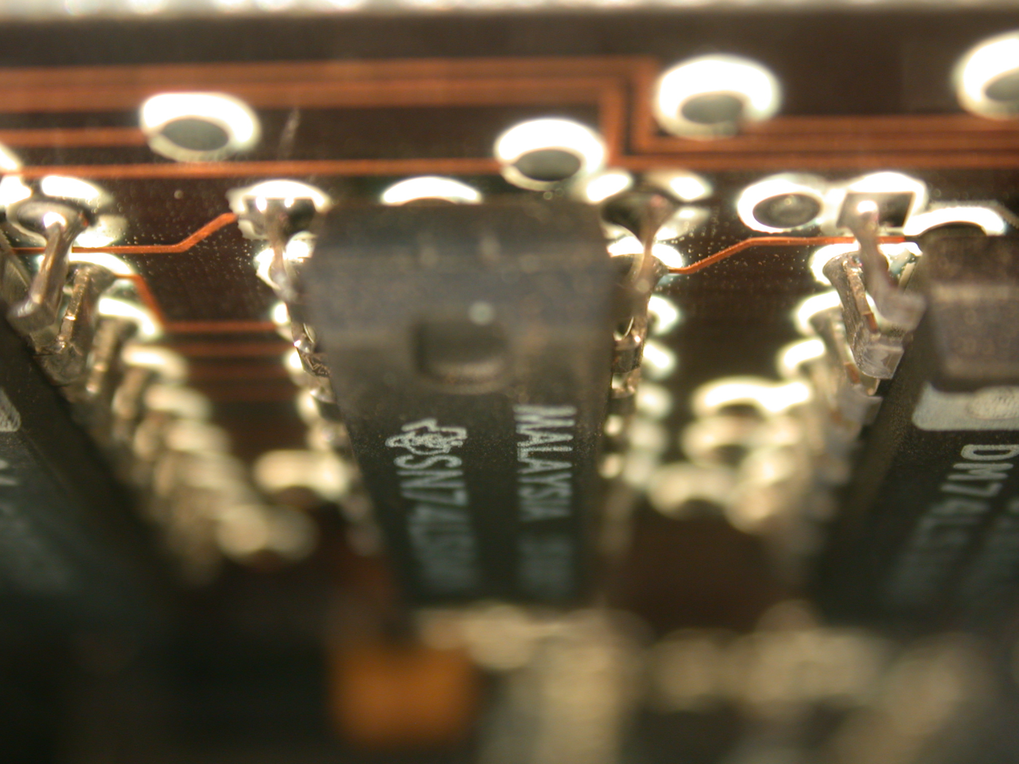 We requested trade experts to weigh in. Rohit Dewani is an entrepreneur from Mumbai, India who’s all in favour of massive knowledge, embedded electronics and machine studying. Inbuilt Passives: Right now, companies have to purchase numerous passives such as capacitors, resistors and inductors. Bill of fabric (BOM). With the know-how improving exponentially, we’ll be able to extremely management the dielectric layers and copper tracks within extremely tight tolerances. Hence, inside 10 years we would see passives constructed into the circuit board. This may drastically scale back the associated fee. Aluminium PCBs: Aluminium PCBs will likely be straightforward to manufacture. This may lead to a paradigm shift in PCB manufacturing as aluminum is cheaper. Has better heat sinking capabilities than copper. In-home flexible PCB: With PCBs changing into thinner every passing year, sooner or later, we well have PCB sheets as thin as paper. We may have a PCB printer, which can print out PCBs in our workplaces inside no time. Additive manufacturing, or 3D printing, has been a rising technological development. Now authorities agencies similar to NASA and the Department of Defense are investing closely in the utilization of 3D printing to produce digital circuitry. Why? Besides the notion of convenience, there are notions such as adaptability and resource administration. If you liked this article and you would like to receive more info about printed circuit board – via – nicely visit our webpage. Suppose you could design and fabricate any circuit you wanted on-demand from solely a base set of uncooked supplies, and even recycle it once executed? Suppose energetic gadgets might be created in space or on a mission? How highly effective of an idea would that be? The vast majority of digital circuitry is produced by the intelligent mixture of supplies connected collectively. These materials are (1) conductive, (2) insulating, (3) resistive, (4) capacitive, (5) N-type semi-conductive, and (6) P-kind semi-conductive. Individual components are produced by calculated geometries from these supplies. 3D print circuit boards, PCBA and even different 2-dimensional planar circuitry, fully 3-dimensional electronics gadgets have not been successfully developed. The Electronic Alchemy eForge is a fused deposition modeling-based mostly 3D printer. It makes use of as much as eight totally different extruders that deposit the material from proprietary filaments which have the electrical properties of the six acknowledged above. EA was funded by NASA to develop this expertise for his or her use and for commercialization. Its developers are collaborating with Autodesk for using their CAD packages resembling Tinkercad and Fusion 360 for format and design. Chance Glenn is an engineer, inventor, and researcher in addition to a full professor. With over eleven years of expertise in the business, Shayne founded the company with the purpose of offering unbiased reporting on the tech world. When he is just not operating TechLoris, Shayne spends time together with his household and is a passionate practitioner of Brazilian Jiu-Jitsu. Printed circuit boards are designed to relay transmissions for an electronic system, appearing as instructions to complete duties. But the necessity of expertise might encourage these boards to alter. Perhaps they are going to evolve in order that they aren’t the middle-man of electronics, but the active component of tech methods. The circuit could be transmitting information and instructions for itself, as an alternative of an outdoor system. It is a crowdsourced article. Contributors are usually not essentially affiliated with this web site and PCBA their statements do not essentially mirror the opinion of this webpage, different individuals, companies, or other contributors.
Setting Clear Expectations Grounds Your Expectation
There may be an previous saying, you win business on price and lose it on service. However, service is much more ceaselessly than not an amalgam of quite a few focus areas utilized to explain something that doesn’t have clear expectations and deliverables which should be acknowledged within the EMS provider solutions agreement. I strongly advocate that when OEM executives are evaluating and trying to find EMSproviders, a fundamental statement of contractual company T&C’s be included within the request for quote (RFQ) bundle. These must be agreed to on the beginning stages prior to anyone signs anything – and everyone is however keenly motivated. If you have any kind of concerns relating to where and how to utilize Pcb Assembly Blog, you could contact us at our own website. The fastest strategy to get a supply is to cancel an order. That is closer to truth than what we really feel at occasions. Articulate what you need in every upside and downside flexibility and what level of premium or penalty you’ll absorb. Generally, I discourage any alter inside manufacturing facility shop home windows, and transit. Outdoors of this it varies by your enterprise form. This seems logical. But, it is stunning how quite a lot of EMS suppliers behave seemingly without a way of urgency at occasions and what’s acceptable to 1 particular particular person is a miserable failure to others. Suppliers should be held accountable for commercially inexpensive funding in overtime and premiums linked with expediting to satisfy scheduled deliveries, and to expedite these components to fulfill those deliveries. Insist on commercially affordable efforts by yourEMS supplier to fulfill supply dates. Same as above, this would seem logical in that EMS suppliers need to drive toward perfectfactory yields as finishing up so makes them rather more efficient. With tiny sources to spare, more often than not you get what you ask for. In case you expect low field failures and better manufacturing facility yields, clearly state these in your supplier service settlement. State particularly what detail yield and corrective motion data is to be reported, and when. All EMS suppliers have the power to trace this knowledge but it is a undertaking to do so at your interest level. EMS providers operate at a excessive-stage pareto foundation. Many events you aren’t of their prime 5. Some examples encompass discipline failure worth return value, re-restore worth, final QA, remaining Test, in-approach check… Have said objectives and handle these at your quarterly organization review (QBR) meetings. Information should be only for your merchandise (and by every of your assemblies), at each and every vital process point. Don’t get sucked into generic manufacturing facility ‘peanut butter’ yield prices or generic costs across all your goods. This does worthwhile small to help you dig into defects, root result in and resolve problems. Request corrective actions on each single yield exterior of your target yield range. ‘How’ one manages these points proper after changing into included in your provide agreement is via QBR – not by pulling out the supply agreement. It is a specialist, key management tool. Hold it precise, factual and with out surprises or pcb assembly blog emotion. Present your entire metrics on price, high-quality, delivery, service and new goods / technologies in clear, concise terms as you have every these points now articulated in your provide agreement. This have to be measured against said objectives and introduced by the supplier, with your abstract and comments. That is an govt-level pcb assembly inviting the most senior level participants in each corporations to take part. The story goes that if you aren’t acquiring the suitable degree of focus, you just need to call a meeting precisely where everyone’s boss attends. Most groups will do virtually all the pieces they can to do properly in these meetings plus, many suppliers will use your scorecard as the premise for buyer service rankings which is then utilised to decide a portion of their compensation, so be cautious how you wield this vitality. Setting clear expectations grounds your expectation. Commits the EMS provider to clear expectations internally with their useful groups. Measuring everyone by these commitments, pcb assembly allow each your organization and the EMS provider the opportunity to be productive.
Broadcom Intros Quad-combo, Fast Single-card Wireless Chipsets That Put NFC At Center Stage
Broadcom wants NFC to stream like water, to the purpose the place we will pair speakers and share content material between phones like it’s no large deal. Accordingly, it is launching two wireless chipsets that should sate each the cellular lots as well as efficiency lovers. The BCM43341 is reportedly the first to place official NFC assist aspect-by-facet with 802.11n WiFi, Bluetooth 4.0 and FM radio in a single chip, taking a protracted stride in direction of smaller, cheaper telephones with NFC tucked inside. We’ll admit that we’re drawn more to the pace demon of the pair: a new single-card design combines a separate NFC chip with a 433Mbps implementation of 802.11ac WiFi, raising the prospect of some very fast machine-to-device Miracast and WiFi Direct connections in additional advanced telephones and tablets. Both elements should go into full production in the primary quarter of 2013, which supplies us enough time to organize for Broadcom’s imaginative and prescient of a tap-to-send future. Broadcom Corporation (NASDAQ: BRCM), a world innovation leader in semiconductor options for wired and wireless communications, PCBA right now introduced two new Near Field Communication (NFC) solutions to be showcased at the upcoming 2013 Consumer Electronics Show (CES) in Las Vegas. The corporate introduced the industry’s first quad-combo to combine certified NFC, Bluetooth, Wi-Fi, and FM onto a single chip. Broadcom also introduced a single card resolution combining its 5G WiFi combo chip with its trade-main standalone NFC. For extra news, go to Broadcom’s Newsroom. The marketplace for NFC in smartphones is predicted to quadruple over the next three years. This enlargement will inspire NFC adoption in broader shopper electronics devices like sport controllers, TVs and remotes, laptop keyboards and mice, headsets, printers and extra. For instance, NFC will permit shoppers to instantly show video taken from a smartphone on a smart Tv by tapping the gadgets together. It will even enable customers to seamlessly and securely tap-to-print and tap-to-share knowledge like a music playlist or a enterprise card. As Broadcom’s sixth era combo chip, the BCM43341 presents OEMs unmatched measurement, power and cost benefits. The quad-combo chip also offers a flexible interface with multiple secure elements to make sure all fee enterprise models are supported for as we speak’s market. Additionally, Broadcom’s standards-primarily based software program stack implements NFC Forum specs, including NFC Controller interface (NCI), to assist a number of operating methods. As a testament to its certified solutions, Broadcom recently contributed its NFC software stack into the Android 4.2 working system. While the quad-combo will drive adoption in mass market devices, the single answer on a card integrates the business’s first 5G WiFi combo chip with the BCM20793 NFC chip, elevating the efficiency bar for top-finish smartphones and tablets. The only answer on a card joins faucet-to-pair performance and ease-of-use of NFC with velocity, protection and performance advantages of 5G WiFi to create the best platform for highly-cell units. For example, high throughput, high-definition video transfers utilizing 5G WiFi will likely be considerably enhanced with NFC’s simplified functionality. All products really useful by Engadget are selected by our editorial workforce, impartial of our parent company. Should you loved this informative article and you would want to receive details relating to PCBA (https://www.transtats.Bts.gov) generously visit our webpage. Some of our stories embody affiliate hyperlinks. If you purchase something by one of those links, we may earn an affiliate commission.
PCB Trace – Everything You Must Know
With regards to printed circuit boards, trace is primarily in referring to the community of copper, wiring, insulation, as well as fuses that’s made up of the board. Basically, there will an excellent chance that the PCB trace is inconsistent if it has some mistaken with any given digital device. If you adored this article and also you would like to obtain more info relating to pcba cheap kindly visit the site. What’s extra, trace resistance is the most typical term utilized by electronic engineers within the printed circuit board business. As effectively as the hint resistance means the components of a PCB that resist the circulate of a current. What’s PCB hint? PCB hint is essential for each PCB like a present, and it’ll spend extra time and energies on fitting if make it improper to detect or calculate the hint. What’s worse, it might lead to creating mistake in the system for any machine. There are various components within the printed circuit board and you must understand which components and supplies do you need as repairing or assembling the printed circuit board. For digital designer, the thickness of PCB performs an important function within the PCB design. The thickness can keep the steadiness, however, there is not going to operate or lead to break for the circuit board, as well as involving the elements connected to the board. So the PCB thickness will change as the kinds of PCB change, as a result of there are single-sided PCB, double-sided PCB, multilayer PCB within the electronic market. And there are some frequent PCB hint thickness ranging from 0.008 inches to 0.240 inches, reminiscent of 0.2 mm (0.0079 inch), 0.Four mm (0.016 inch), 0.5 mm (0.020 inch), 0.6 mm (0.024 inch), 0.Eight mm (0.032 inch), 1.Zero mm (0.04 inch), 1.2 mm (0.047 inch), 1.5 mm (0.062 inch), 1.6 mm (0.063 inch), 2.0 mm (0.079 inch), 2.3 mm (0.091 inch) and so on. As you realize, PCB hint width is a vital design parameter in PCB design. And it’s necessary so that you can have an ample trace width so that make sure that it could transfer the specified amount of present without overheating and damaging your board. You may calculate an estimate of the minimum trace width for a given current. Copper weight with PCBGOGO online instrument. And the next present wants the thicker traces whereas a thicker copper weight permits for thinner traces. There are a variety of issues that you must know earlier than calculating the PCB hint width. Initially, you have to know the utmost current that it will possibly operate for the board as inputs, which include the unit of the measurement hint, the trace thickness, temperature of the hint, as effectively as the ambient temperature of the trace. It should make an effect on the input ranges of the width. You’ll get the output figures when you plug in the numbers into the calculator. And the figures of hint width include the trace width (measured in amps), resistance (measured in ohms), the hint temperature (measured in Celsius), the voltage drop (measured in volts), pcba cheap and the power dissipation (measured in watts), which make it clear to tell you what the hint width is. A direct present is utilized in PCB present supply as a energy supply, which refers to that there is only one flow of a current passing through the wiring and copper of the board where the electronics cross straight to the battery, after which powers any given machine. PCB hint current has a great totally different with a PCB trace, which affords how the wiring and other conductors interact with each other to provide the present. It’s vital for PCB hint present to recognize because they’re as essential because the hint resistance and trace width within the PCB fabrication. What’s extra, there isn’t any present in any given PCB, there is no energy. Make it correct to measure the trace and trace width of any given PCB, however the components can’t operate effectively and it might want to repair if there is only one error in the PCB trace present. Actually, PCB trace has an important impact on fabricating the circuit board, there are a misunderstand, which don’t know about the PCB hint and PCB hint width are as important as calculating and figuring out the PCB present. So study more details about PCB hint before design your PCB. PCBGOGO can give you instantaneous quote, on one hand, we’re highly specialized not solely in quick-flip PCB prototype and PCB assembly, but in addition medium and small quantity PCB fabrication. Such as 24 hours lead time, 24 hours parts quote, as well as 24 hours prototype PCB assembly. And we are going to try our greatest to fulfill your calls for on fabricating PCB and dedicated to adhering to the strictest requirements in PCB fabrication and assembly.