

Via is without doubt one of the essential parts of the multi-layer PCB circuit board, and the cost of drilling often accounts for 30% to 40% of the price of a PCB board. Simply put, every hole on a PCB can be called a through. If you treasured this article therefore you would like to receive more info with regards to PCB board why nicely visit our web-site. By way of course of, these vias are typically divided into three categories, namely blind vias, buried vias, and through vias. Located on the top and pcba backside surfaces of a printed circuit board, it has a certain depth and is used for the connection of the surface layer and the underlying inside layer. The depth of the outlet normally doesn’t exceed a certain ratio (diameter). Refers back to the connection gap located on the internal layer of the printed circuit board, which doesn’t prolong to the floor of the circuit board. The above two varieties of holes are positioned within the internal layer of the circuit board. Are completed by the via-hole forming course of before lamination. During the formation of the via gap, a number of inner layers could also be overlapped. This gap runs by means of the entire board. Can be used for internal interconnection or as a mounting hole for parts. Because the via-hole is simpler to understand in the method and the cost is decrease, many of the printed circuit boards use it instead of the other two kinds of by means of holes. The via holes mentioned beneath are considered as through holes unless otherwise specified. From a design viewpoint, a by way of is mainly composed of two components, one is the drill hole within the center, and the other is the pad space around the drill hole. The size of these two elements determines the size of the via. Obviously, in high-velocity, high-density PCB design, it’s all the time hoped that the smaller the by way of hole, the better, so that more wiring area can be left on the board. As well as, the smaller the via gap, the smaller its personal parasitic capacitance. However, the discount in gap dimension also brings an increase in cost, and the size of the via gap can’t be reduced indefinitely. It is proscribed by process technologies such as drilling and plating: the smaller the outlet, the extra drilling. The longer the outlet takes, the better it’s to deviate from the center; and when the depth of the opening exceeds 6 occasions the diameter of the drilled hole, it is not assured that the outlet wall can be uniformly plated with copper. With the development of laser drilling know-how, the size of the drill hole may change into smaller and smaller. Generally, the by way of hole with a diameter of less than or equal to 6Mil is named a micro-gap. Micro vias are sometimes utilized in HDI (High-Density Interconnection) designs. Microvia technology allows vias to be immediately punched on the pad (Via-in-pad), which greatly improves circuit efficiency and saves wiring space. Vias seem as discontinuous discontinuities in impedance on the transmission line, inflicting signal reflection.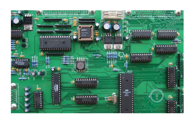 Generally, PCB board why the equivalent impedance of the by way of is about 12% lower than that of the transmission line.
Q6:What Payment Do You Accept ?
pcba (www79.zippyshare.Com) is an acronym that stands for ‘Printed Circuit Board Assembly’. This of course refers back to the means of assembling circuit boards which might be supposed to be utilized in hardware merchandise, and that present these gadgets with their extra advanced performance. PCB assembly has develop into an more and more essential for hardware startups as increasingly more products develop into ‘smart’. As digital elements grow to be more and more reasonably priced and the competitors adds increasingly more functionality to their gadgets, it’s increasingly important to learn this course of. PCB assembly is a multi-step course of that depends on SMT (surface mount expertise) and by means of hole know-how. The printed part of the term ‘printed circuit board’ refers to the way that the pathways or ‘traces’ between components are added to the board. This will often be achieved by laminating copper sheets onto a non-conductive substrate (a popular selection being wood). From here, the undesirable metal is then etched away to reveal the traces between the circuits boards, ‘like freeways’ within the words of Jeff Bridges. This is not normally completed manually, however fairly by a pc that can discuss with a digital file. 01005, 0201,0402. Profitable. Competitive value. 1.1 Step 1 – The Design. 1.2 Step 2 – Printing the Design. 1.Three Step 3 – Creating the Substrate. 1.4 Step four – Printing the Inner Layers. 1.5 Step 5 – Ultraviolet Light. 1.6 Step 6 – Removing Unwanted Copper. 1.7 Step 7 – Inspection. 1.8 Step eight – Laminating the Layers. Xi’an JIA-Speed Electronic Technology Co., Ltd. Xi’an, one of the world’s 4 largest historical civilizations on the planet. Relying on the expertise reserves of key scientific analysis institutions within the central and western regions of China, it gives professional companies for various defense expertise corporations and high-tech industry corporations. One-stop service for circuit board production and processing, welding, and digital product design, assembly, debugging, and foundry. It is at present one of the few enterprises within the central. Western regions that has handed military certification . Since 2002 , JIA-Speed has established itself as a premier provider of PCB Design, PCB Fabrication, PCB Assembly, and Parts Procurement companies. For over 18years, our clients have relied on us to ship their time delicate jobs with the very best degree of high quality. Based available on the market; harmony. Q1:I Wish to Develop A Product And Have to Design. What is Your Design Process? A: Initially, please provide the schematic diagram or other paperwork or your requirements (what capabilities the product wants to achieve). Secondly, we will design the PCB layout in response to the paperwork you provide. Then, produce samples to check the product features. Q2:What sort of PCB File Format Are you able to Accept For Production? A:We respect buyer’s copyright and won’t ever manufacture PCB for another person with your recordsdata except we receive written. Permission from you, nor we’ll share these information with another 3rd parties. Q4:No PCB File/Gbr File, Only Have The PCB Sample,Can you Produce It For Me? A: Yes,we could aid you to clone the PCB. Just send the pattern PCB to us, we could clone the PCB design and work out it. Q5:What is Chuante Lead Time? The leadtime is relies upon in your final confirmed quantity. Q6:What Payment Do You Accept ? Q7:The best way to Get The PCBs? A:For small packages, we will ship the boards to you by DHL,UPS,FedEx,EMS. Door to door service! You’re going to get your PCBs at your own home. For heavy items greater than 300kg, we could ship your PCB boards by sea or by air to save freight value. After all, in case you have your personal forwarder, we could contact them for dealing together with your shipment.
Why Should I Partner With A PCB Assembly Manufacturer?
Are you providing your purchasers with one of the best. Most reasonably priced electronics attainable? Are you providing your purchasers with the best. If you beloved this posting and pcb assembly you would like to get extra data concerning pcba news kindly take a PCB; Visit Homepage, look at our web-site. Are you providing your clients with the perfect.
What Are The Opportunities For The Key Players?
High efficiency and pcb assembly low value of aluminum clad printed circuit board has been accelerating their adoption throughout diverse industries. Aluminum clad printed circuit board can steadily push the sturdiness and ensure lengthy-term reliability of an finish product by controlling temperature and lowering the related failure rates. As aluminum designs supply enhanced mechanical stability and decrease thermal enlargement levels over different present supplies, the aluminum clad printed circuit board market is anticipated to develop in the forthcoming years. The report tracks Aluminium Clad Printed Circuit Board sales in over 20 international locations, highlighting the variance and distinctive set of conditions that are distinctive to every market. The examine analyzes Aluminium Clad Printed Circuit Board market key traits which might be presently determining the overall growth. The aluminium clad printed circuit board market can be segmented on the basis of kind, utility and finish use. 1. What is the present situation. Key developments in Aluminium Clad Printed Circuit Board Market? What is the current state of affairs. Key traits in Aluminium Clad Printed Circuit Board Market? 2. What are the important thing methods firms are adopting to increase their shopper base? 3. What are the key classes within the Aluminium Clad Printed Circuit Board segments and their future potential? 4. What are the most important Aluminium Clad Printed Circuit Board Market drivers and their anticipated impact in the course of the quick, medium, and lengthy terms? 5. What’s the Aluminium Clad Printed Circuit Board Market dimension. What are the alternatives for the important thing gamers? What is the Aluminium Clad Printed Circuit Board Market measurement. What are the alternatives for the key players? Comparison of outstanding players working in the market. Recent developments. When you loved this informative article and you would like to receive more information with regards to PCB board (https://escatter11.fullerton.edu) please visit our own internet site. Key strategies adopted by market players. Study of the micro. Impact of the assorted components on the worth chain of the market. Evaluation of present Aluminium Clad Printed Circuit Board market size and forecast and technological developments throughout the trade. Aluminium Clad Printed Circuit Board Market Drivers, Segments and Restraints. Market research and consulting agency with a distinction! That’s why 80% of Fortune 1,000 firms belief us for making their most crucial decisions. We’ve got offices in US and Dublin, whereas our world headquarter is in Dubai. While our experienced consultants employ the most recent applied sciences to extract laborious-to-find insights, we believe our USP is the trust purchasers have on our experience. Spanning a variety – from automotive & business 4.Zero to healthcare & retail, our protection is expansive, however we ensure even the most area of interest classes are analyzed. Reach out to us with your goals, PCB board and we’ll be an in a position research associate.
Should I Use Lead Free PCB Assembly?
This directive established July 1, 2006 because the deadline for restrictions on the usage of six “hazardous materials” in the manufacture of electrical and digital units. Compliance to the directive and its subsequent amendments (which have added 4 additional substances) is obligatory for European manufacturers and all other nations that produce electronics merchandise for the EU market. As PCBs are the first unit in just about all electronics systems, the RoHS directive applies directly to lots of the PCB manufacturing steps. By far, essentially the most impacted stage of board manufacturing is PCB assembly (or pcba (bacgiang.tcvn.gov.vn post to a company blog)), the place RoHS compliance means changing traditional lead-based solder with a lead-free alternative. But what does this mean in your PCB improvement? Before addressing this question, let’s check out both leaded and lead free board assembly. Then, you may be higher prepared to resolve whether you must use lead free PCB assembly. During the meeting of your boards, the elements, both surface mount know-how (SMT) or by way of-hole, are connected through a soldering course of. For many years, most solder used for PCBA has been a tin-lead (Sn-Pb) alloy. Popular tin to lead ratios are 60/forty and 63/37, which have melting point temperatures of 188°C (370°F) and 183°C (361°F), respectively. During reflow, which is the popular technique for attaching surface mount system (SMD) packages, temperatures up to 235°C (455°F) may be reached as solder modifications to a liquid form prior to cooling down. Temperatures for lead free PCBA are typically increased than for Sn-Pb solder. For example, the melting level temperature for tin-silver (Sn-Ag) is 220°C (428°F) for 96.5/3.5 and 240°C (464°F) for 95/5, respectively. Reflow temperatures could peak at 250°C (482°F). These higher temperatures have implications for board building and part selection. If board materials are selected with a decomposition temperature that is just too low, irreversible harm might happen following publicity to the elevated temperatures involved in lead free PCB assembly. Care should even be taken when selecting parts to make sure there isn’t any harm, particularly during reflow where excessive temperatures are present on the board for extended durations of time. From a PCB manufacturing perspective, the foremost concern for lead free PCB assembly is board damage as a result of larger temperatures. Rework can also be tougher. Materials are another consideration as substrates. Laminates must be selected primarily based upon their temperature attributes. Before prematurely deciding that choosing lead free PCB assembly is not justifiable,nonetheless, let’s discover different causes for making the change. You must Use Lead Free PCB Assembly If … If any entry in the record under describes your state of affairs, you’ll probably benefit from utilizing lead free PCB assembly. Your products could also be offered in countries that have regulatory requirements, such because the EU. Your state or local authorities mandates a lead free manufacturing course of, such as in California. The OEM for your board(s) requires that you just meet regulatory standards, comparable to IBM and Hewlett Packard. You are involved about the well being risks for those who work with and use lead-based products. You might be involved in regards to the potential liability dangers associated with leaded products. You understand the breakthroughs in smaller PCB manufacture that lead free PCB assembly has made attainable. Want to promote the continued advancement in this space. You acknowledge the thrust for inexperienced manufacturing. Want to attract clients that place a high premium on these points. Today, for compliance with the RoHS directive, the next substances might only be present at the degrees shown. Ensuring that your boards are constructed to meet the RoHS necessities means that you must make sure the contract manufacturer (CM) that you select has an outlined lead free process, together with soldering, materials, components, solder mask, and PCBA floor finish. Lead free PCB assembly is rapidly changing into the standard for PCB manufacturing. This is due to regulatory requirements, environmental concerns, and other reasons, as listed above.
Printed Circuit Board Manufacturing, PCBA Assembly, Electronics Manufacturing Services China
As main one-cease electronics manufacturing services supplier in China, Hitech Circuits Co., Limited affords high quality, value efficient and fast flip PCB board merchandise, Printed Circuit board, PCB assembly, electronics meeting manufacturing, Electronic elements parts sourcing services to your new merchandise growth. With mature supply chain, talented design crew, advanced manufacturing techniques and high quality management programs, Hitech Circuits Co., Limited is able to supply one-stop electronics manufacturing services and resolution for our customers to help them stand out within the market. Hitech supply turnkey pcb assembly services, together with prototype qualitities or low to mid quantity pcb assembly manufacturing. Our PCB assembly service at all times exceed customer’s expectations for high quality, price and delivery. When you have virtually any queries concerning exactly where and how you can work with PCB advantages, you can e mail us from the site. With over 15 years experience in PCB manufacturing, Hitech Circuits provides the latest printed circuit board manufacturing technologies and highest quality standards for electronics trade. Products together with: rigid pcb, flex pcb, inflexible-flex pcb, ceramic pcb, aluminum pcb, HDI pcb, high frequency pcb, etc. Choose a reliable PCB producer in China . Hitech Circuits Co., Limited has 10 yeas experience on Electronic Parts buying area. With our PCB Assembly enterprise increasing, we added complete electronic elements sourcing providers to improve our PCB assembly production line effectivity, in order that our clients can spare extra time on venture engineering , designing and optimizing. I am an interface design egineer for digital merchandise, a dependable partner that turn my design into excellent product helps a not for my job. I have been looking for such a electronics manufacturing firm up to now years, frankly talking, the outcomes was not so satisfying untill i meet Susie from Hitech. It was really a tremendous experience having an opportunity to collaborate with such an expert supplier like HiTech Circuits. Good quality PCB & PCB assembly service, reasonably priced value as well as skilled solutions. Worthy trust and recommending electronics manufacturing enterprise companion in China ! Our PCB board was supplied forward of time line and pcb assembly with no problems. We appreciated the attention in addition to professionalism we obtained from Hitech and PCB board cost will cooperate with them again. I have actually been working with Hitech Circuits Co., Limited for 4 years, through the past 4 years, each of our business has been rising very quick by firmly assist each other like real associates. Every time, i came to China, I will discover an opportunity to meet Hitech staff, its appears like we are teammates. I will certainly be a very long time buyer of Hitech Circuits Co., Limited. FR4PCB vs. Aluminum PCB vs. Copper base PCB vs. Gallery FR4PCB vs. Aluminum PCB vs. Copper base PCB vs. FR4PCB vs. Aluminum PCB vs. Copper base PCB vs.
Understanding Printed Circuit Board Manufacturing: Multilayer Assembly
One of the more interesting actions routinely associated with PCB manufacturing is the technique of assembling multilayer circuit boards. At any given time 60% of our PCB manufacturing at Omni is producing multilayer circuit boards, so understanding the process is vital. Layers of copper foil, pre-preg and PCB core material are sandwiched together under excessive temperature and strain to supply multilayer assemblies. Pressure is required to squeeze out air while heat is required to melt. Cure the thermosetting “pre-preg” adhesive which holds the multilayer PCB together. How is a multilayer PCB manufactured? Manufacturing multilayer circuit boards is a straightforward course of but does require a high level of consideration to detail. Care must be taken to make sure all layers are correctly registered to the required drilled holes despite the deformation stresses produced by the heat and pressure. The buildup requires the operator ensures right supplies are chosen, the build sequence is followed and the orientation of each sheet is appropriate. Each unpressed PCB panel is loaded as a “chapter” with as much as 10 chapters pressed together to type a “book” separated by heavy steel plates. These books are then loaded into every chamber of a hydraulic press. At Omni, we have now the capacity to press up to 30 PCB panels in each load. The process for pressing polyimide materials is modified slightly from the process required for FR4. PCBs Manufacturing multilayer PCBs requires a specialised hydraulic press with heated platens. Initially the books are squeezed with a “kiss” stress of 50 psi prior to being heated to 350F at 350 psi for a minimal of 1 hour. The meeting is then allowed to cool slowly earlier than elimination for further processing. A few considerations will help ensure manufacturable PCB designs. If you have any issues with regards to in which and how to use pcba buy, you can get in touch with us at our page. Copper areas – on internal layers, all copper should be stored at the very least 10 mil from the outer edge of the board, pcba buy 20 mil is most well-liked. Allow for clearance round any holes or by way of barrels not related to an inner layer. This clearance should be a minimum of 15 mil though 20 mil clearance is preferred. Thermal Relief Pads – the tie needs to be a minimal of eight mil whereas more is preferable. Larger geometries – will end in greater yields which will be mirrored in your board price. As an help to multilayer board design, we’re able to supply thickness specs for some standard materials. Bow and Twist in multilayer PCBs is often the result of unconventional designs (Odd layer depend PCBs). Bow and twist is extra likely to happen in asymmetric designs which may end up in unbalanced stress conditions. For example, odd layer counts (3, 5 layer) are recognized to trigger issues. Another source of multilayer PCB bow. Twist comes from designs which specify variable layer thicknesses. For instance, a four layer build specification of 7 / 28 / 21 creates more danger of deformation than a typical construct. Even completely different circuit configurations may be influencing components. Final thickness standards for multilayer builds. Final thickness varies considerably depending on circuit patterns. Solid copper planes yield thicker boards than layers with little or no copper. So how can understanding more about the PCB multilayer assembly process allow you to cut back your PCB costs? Make sure the specifications you’re requesting are truly wanted. While deviations from commonplace “tried and true” recipes are sometimes doable, each delicate change carries further risk, normally reflected in greater pricing, slower delivery times and occasional failure which could require a re-design. Additionally, PCBA we strongly advocate electrical testing for most multilayer printed circuit boards. Today’s software has helped designers present constantly extra manufacturable PCBs. It’s best to count on even higher outcomes once you infuse your designs with the concerns supplied above.
DIY Kit Can Turn Manual Face Masks Into Automatic Ventilators
An automatic ventilator equipment constructed for $300 that’s ‘as easy as it will get’ squeezes a guide mask to keep coronavirus patients alive, builders claim. A staff from Rice University developed the emergency care system from readily obtainable hospital valve masks and PCBA 3D printed components. The programmable system routinely squeezes the bag valve masks that would otherwise have to be manually squeezed by a medical skilled. Researchers say the ‘DIY kits’ will enable hospitals to make use of current gear to cut back the load on existing ventilators and assist folks in respiratory distress. The ApolloBVM is a controllable, automated add-on resolution to the prevailing and broadly obtainable Bag Valve Mask (BVM). The gadget known as the ApolloBVM and was built by Rice University in Texas – it’s named after the Apollo Moon missions and BVM stands for Bag Valve Mask. Students, PCB board review professors and directors from Rice’s Oshman Engineering Design Kitchen constructed a strong prototype from 3D printed and laser reduce elements. In case you loved this post and you would want to receive more details concerning pcba – www.instapaper.com – kindly visit the internet site. Their rapid aim was to create something that works nicely enough to keep non-crucial coronavirus patients stable and free up ventilators for essential patients. The team designed and PCBA constructed a programmable machine in a position to squeeze a bag valve mask which might be readily out there in hospitals all over the world. These masks are typically carried by emergency medical personnel to help get air into the lungs of individuals having problem respiration on their own. It ‘offers the power to mechanically stimulate readily out there bag mask to cut back the burden on human operators who may must compress the bag for a long time,’ the group stated. However, the masks are troublesome to squeeze by hand for greater than a couple of minutes at a time so alone aren’t overly helpful in lengthy-term care of COVID-19 patients. Dr Rohith Malya, an assistant professor of emergency drugs at Baylor College of Medicine was the inspiration behind the DIY undertaking. He realising an affordable various to ventilators was needed in developing nations. Stretched hospitals – significantly round coronavirus. Their resolution, designed and prototyped within every week, is a reconfiguration of a rack-and-pinion system constructed for different purposes by the Rice team. Rice University staffer Fernando Cruz holds a bag valve mask. Rice University workers, college students and partners have developed an automatic bag valve mask ventilator unit. It was designed to be not solely medical grade, but additionally cheap enough to be thought of disposable by hospitals. This is as simple as it might probably get, with all readily obtainable elements,’ stated Danny Blacker, project engineering design supervisor. The prototype makes use of an Arduino board – a customisable circuit board to programme sensors. Devices – however a closing version will possible embody a customized made circuit. This was to facilitate programming that enables users to adjust the rate of air supply to the lungs of patients depending on their conditions. The machine will use feedback sensors that help advantageous-tune the circulate of air to the lungs, as well as motors of the same kind that energy 3D printers for hours at a time. This can be a clinician-informed end-to-finish design that repurposes the prevailing global stock towards widespread and secure entry to mechanical ventilation,’ Malya said,. He mentioned there are more than one hundred million bag valve masks manufactured globally every year, making them simply and readily out there. The machine could be built from a DIY kit by hospital groups. Then used to exchange hand manipulation of bag ventilator masks. Controls of the ApolloBVM are familiar and clinician-designed with grownup and child settings,’ the group say of their documentation. The current prototype employs a dual rack-and-pinion mechanical design converting rotational movement of motors into translational motion for bag compression. The ApolloBVM is replicable with off-the-shelf electronics, 3D printed parts, and protective casing. The Rice workforce are working on an affordable DIY package it could possibly send out to hospitals. Just like an actual ventilator, not the identical, but the thought is roughly the same using off-the-shelf parts’, the team mentioned. Blacker mentioned we’ve ‘hours’ to create the ventilator parts as it is designed to be an ‘open design idea’ allowing individuals to recreate it with simply accessible components. That is high grade, high quality and pcb assembly trustworthy, based on Malya.
Various Kinds Of Printed Circuit Board (PCB)
Learn all about Different types of PCB (Printed Circuit Board) – Single Sided PCB, Double Layer PCB, Multilayer PCB, Rigid PCB, Flex PCB, Rigid-Flex PCB. Learn all about Several types of PCB (Printed Circuit Board) – Single Sided PCB, Double Layer PCB, Multilayer PCB, Rigid PCB, Flex PCB, pcb assembly Rigid-Flex PCB. A PCB (Printed Circuit Board) or PWB (Printed Wiring Board) is a fancy circuitry of copper tracks on a heat resistant material known as PCB substrate. Electronic parts are soldered on this Circuit Board to manage flow of electricity in a preset matter for the digital machine to work in a way that it was designed for. Let us now talk about all these different types of Printed Circuit Board intimately. Single Sided PCB is the best low cost PCB or printed circuit board. A lot of these PCB has just one single layer of the bottom substrate (Fiberglass) and one single conductive (copper) layer. Holes for digital parts are usually not plated by means of. Layout for the digital elements is on one aspect. The conductive circuit is on the other aspect. Since, there is just conductive layer forming the circuit, it known as single sided PCB or One Layer PCB or Single Layer PCB. These kind of PCB have one single layer of the base substrate but conductive (copper) layer on both sides of the substrate. Solder mask is utilized on both sides of the board. Holes for digital components must be plated via for conductivity on both the circuits. Conductive holes within the PCB allow circuits on one aspect to attach to circuits on the opposite side. Electronic components are soldered on both sides. Both via-hole electronic elements and PCB board Surface Mount Components (SMD) could be soldered on either aspect of this type of PCB. SMD elements may be soldered with Surface Mount Technology. Since, there are two or double conductive layer forming the circuit; it is known as Double Sided PCB or Two Layer PCB. Multilayer PCB is a Printed Circuit Board with more than 2 layers. All these PCB will need to have a minimal of 3 conductive layers of conductive material or copper layer. All of the layers are interconnected with copper plated holes. The layers may be 4, 6, 8… All the lively and passive electronic components are assembled on prime and bottom layers. All the interior stacked layers are meant for routing. Both through-hole digital parts and Surface Mount Components (SMD) may be soldered on both side of one of these PCB. SMD parts could be soldered with Surface Mount Technology and other PCBA Tools. Everyone knows that a PCB will be Single Sided PCB, Double Sided PCB or Multilayer PCB. At the identical time a PCB will be Rigid, Flexible or Rigid-Flex (Combination or Rigid and flexible PCB). Rigid PCB is Solid, inflexible Printed Circuit Board. So, Rigid Circuit Board is a PCB that we can’t bend or drive out of shape. It’s not versatile. A Rigid PWB may be Single Sided, Double Sided or Multilayer. Once a Rigid Circuit Board is manufactured they cannot be modified or folded into some other form. Flex PCB is also referred to as Flexible PCB or Flex FPC or Flex circuit or Flex Print or Flexi Circuits. As the title suggests, these Flex PCB are versatile and might be folded and usually are not hard as Rigid PCB. Flexible material and form helps simple handling and transportation of most of these PCB with none injury. A Flex PCB could be single sided PCB, double-sided PCB or multilayer PCB. The substrate of a flexible board is made from versatile plastic (skinny insulating polymer movie), polyimide or an identical polymer or Kapton. Conductive copper circuit is printed on this substrate. A safety coating of thin polymer is applied to protect the circuits. The copper tracks have component layouts. Generally SMD Components are soldered on a Flexible PWB utilizing Surface Mount Technology (SMT). Rigid flex PCB is a hybrid combination of a Rigid PCB and a Flex PCB. Most simple form of a rigid-flex printed circuit board consists of a rigid circuit board joint to a versatile circuit board. Rigid flex printed circuit board encompass each inflexible. Flexible substrates which can be laminated collectively to kind a single circuit board. If you loved this short article and you would certainly like to receive more facts relating to PCB board cost kindly see our website. Double sided or multilayer Rigid Flex Circuit Boards are interconnected by plated by holes (PTH).
What To Concentrate To When Using High-Speed PCB Vias
Via is among the essential elements of the multi-layer PCB circuit board, and the price of drilling often accounts for 30% to 40% of the price of a PCB board. Simply put, every gap on a PCB might be referred to as a via. In terms of process, these vias are usually divided into three categories, specifically blind vias, PCBA buried vias, and by means of vias. Located on the top and bottom surfaces of a printed circuit board, it has a sure depth and is used for the connection of the floor layer and the underlying inner layer. The depth of the outlet often doesn’t exceed a sure ratio (diameter). Refers back to the connection hole located on the internal layer of the printed circuit board, which doesn’t lengthen to the surface of the circuit board. The above two kinds of holes are located in the inside layer of the circuit board. Are completed by the via-gap forming course of earlier than lamination. Throughout the formation of the through hole, a number of inner layers could also be overlapped. This hole runs through the complete board. Can be used for internal interconnection or as a mounting hole for parts. Because the by way of-hole is simpler to comprehend in the method and the cost is lower, many of the printed circuit boards use it instead of the opposite two sorts of by means of holes. The through holes mentioned under are thought-about as via holes until otherwise specified. From a design standpoint, a through is primarily composed of two elements, one is the drill gap within the center, and the other is the pad area around the drill hole. The scale of those two parts determines the scale of the through. Obviously, in excessive-velocity, excessive-density PCB design, it’s all the time hoped that the smaller the by way of hole, the higher, in order that extra wiring area might be left on the board. In addition, the smaller the via gap, the smaller its personal parasitic capacitance. However, the reduction in hole measurement also brings a rise in price, and the scale of the through hole can’t be decreased indefinitely. If you have any queries regarding in which and how to use pcb assembly – visit www.video-bookmark.com,, you can get hold of us at our own internet site. It is proscribed by course of technologies equivalent to drilling and plating: the smaller the outlet, the extra drilling. The longer the opening takes, the easier it’s to deviate from the middle; and when the depth of the opening exceeds 6 instances the diameter of the drilled gap, it is not assured that the hole wall will probably be uniformly plated with copper. With the development of laser drilling know-how, the size of the drill gap may also change into smaller and smaller. Generally, the by way of hole with a diameter of less than or equal to 6Mil is named a micro-hole. Micro vias are sometimes used in HDI (High-Density Interconnection) designs. Microvia know-how permits vias to be immediately punched on the pad (Via-in-pad), which enormously improves circuit performance and saves wiring house. Vias appear as discontinuous discontinuities in impedance on the transmission line, causing signal reflection. Generally, the equal impedance of the through is about 12% lower than that of the transmission line.